
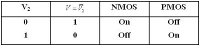
The CMOS logic gate can be conceptually modeled by the circuit in Fig 3.1, in which the position of the two switches is controlled by the input voltage vi. The circuit is designed so there will never be a conducting path between the positive and negative power supplied under steady –state conditions. When the NMOS transistor is on, the PMOS transistor is off; if the PMOS transistor is on, the NMOS device is off.

Fig 3.1. Inverter circuit diagram


In the CMOS inverter of Fig 3.1, the source of the PMOS transistor is connected to VDD , the source of the NMOS transistor is connected to VSS (0 V in this case), and the drain terminals of the two MOSFETs are connected together to form the output node. Also the substrates of both the NMOS and PMOS transistors are connected to their respective sources, and so body effect is eliminated in both devices.

(a)

(b)
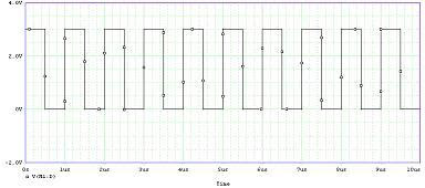
Fig 3.2. Inverter input output voltages, (a) Input voltage. (b) Output voltage
Table 3.1 CMOS Inverter truth table and transistor states

CMOS Voltage Transfer characteristics
Figure 3.3 shows the voltage transfer characteristic (VTC) of the Symmetrical CMOS inverter, designed with Kp=KN . The VTC can be divided into five different regions, as shown in the figure and summarized in table 3.2. For an input voltage less than VTN = 1V in region 1, the NMOS transistor is off, and the output is maintained at VOH = 5V by the PMOS device.
Similarly, for an input voltage greater than (VDD - | VTP | )(4 V) in region 5, the PMOS device is off, and the output is maintained at V0L = 0V by the NMOS transistor. In region 2, the NMOS transistor is saturated, and the PMOS transistor is in the linear region. In region 3, both transistors are saturated. The boundary between regions 2&3 defined by the boundary between the saturation and linear region of operation for the PMOS transistor. Saturation of the PMOS device requires:

Table 3.2 Regions of operation of transistors in a symmetrical CMOS inverter

In a similar manner, the boundary between regions 3 and 4 is defined by saturation of the NMOS device:

In region 4, the voltage place the NMOS transistor in the linear region, and the PMOS transistor remains saturated. Finally, for the input voltage near VDD/2 (region 3), both transistors are operating in the saturation region.
By using small channel length, produce increase in cut – off frequency so delay time decreased and this increase speed of operation.

Also me advantages of using small channel length:
1- decreasing tsohreshold voltage
2- decreasing supply voltage
3- decreasing palter dissipation
