Custom Search
Showing posts with label Design and Simulation of Differential and Multistage Amplifiers. Show all posts

Wednesday, May 11, 2011

Operation with a DiFFerential Input Voltage


Next we apply a difference or differential input voltage by grounding the gate of Q2  (i.e.,setting vG2 = 0) and applying a signal vid to the gate of Q1 as shown in Fig. 2.3. It is easy to see that since vid=vGS1-vGS2 , if vid is positive, VGSl will be greater than vGs2 and hence iD1 will be greater than iD2 and the difference output voltage (vD2-vD2) will be positive. On the other hand, when vid is negative, vGS1 will be lower than vGS2 , iD1 will be smaller than iD2, and correspondingly vD1 will be higher than vD2; in other words, the difference or differential output voltage (vD2-vD1) will be negative.
The MOS differential pair with a differential input signal

Fig. 2.3  The MOS differential pair with a differential input signal vid applied. With vid  positive: vGS1 > vGS2 , and vD1<vD2 thus thus (vD2-vD1) will be positive. With vid negative: vGS1 < vGS2, iD1< iD2 and (vD1>vD2­ ) thus (vD2-vD1) will be negative.

From the above, we see that the differential pair responds to difference-mode or differential input signals by providing a corresponding differential output signal between the two drains. At this point, it is useful to inquire about the value of vid that causes the entire bias current I to flow in one of the two transistors. In the positive direction, this happens when vGS1 reaches the value that corresponds to   iD1= I, and vGS2 is reduced to a value equal to the threshold voltage Vt, at which point vs=-Vt The value of vGS1 can be found from


where VOV  is the overdrive voltage corresponding to a drain current of 1/2 (Eq. 2.5). Thus the value of vid at which the entire bias current I is steered into Q1 إس

if vid is increased beyond  
 , iD1 remains equal to I, vGS1 remains equal to
, and vS rises correspondingly, thus keeping Q2 off. In a similar manner we can show that in the negative direction, as vid  reaches 
 ,Q1 turns off and Q2 conducts the entire bias current I.
Thus the current I can be steered from one transistor to the other by varying vid din the range
  
 
which defines the range of differential-mode operation. Finally, observe that we have assumed that Q1 and Q2 remain in saturation even when one of them is conducting the entire current I.
To use the differential pair as a linear amplifier, we keep the differential input signal vid small. As a result, the current in one of the transistors (Q1   when vid is positive) will increase by an increment  
 proportional to vid  to
Simultaneously, the current in the other transistor will decrease by the same amount to become    
A voltage signal 
 develops at one of the drains and an opposite-polarity signal, 
, develops at the other drain. Thus the output voltage taken between the two drains will be 
 , which is proportional to the differential input signal vid. The small-signal operation of the differential pair .

The MOSFET differential pair for the purpose of deriving the transfer      characteristics
 
FIGURE 2.5 The MOSFET differential pair for the purpose of deriving the transfer      characteristics, iD1 and iD1 versus vid=vG1 -vG2 .
" Operation with a DiFFerential Input Voltage " !

Operation with a Common-Mode Input voltage

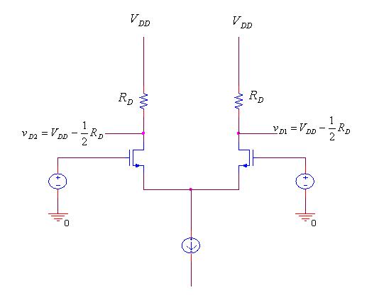
To see how the differential pair works, consider first the case of the two gate terminals 
interjoined together and connected to a voltage vCM called the common-mode voltage. That is as shown in Fig (2.2)                
 
Since Ql and Q2 are matched, it follows from symmetry that the current I will divide equally between the two transistors. Thus
and the voltage at the sources, vs will be

 
where VGS is the gate-to-source voltage corresponding to a drain current of I/2. Neglecting channel-length modulation, VGs and I/2 are related by


or in terms of the overdrive voltage   
  
                                                                                                                             
The voltage at each drain will be

Thus, the difference in voltage between the two drains will be zero.

The MOS differential pair with a common-mode input voltage
Fig. 2.2      The MOS differential pair with a common-mode input voltage

Now, let us vary the value of the common-mode voltage vCM Obviously, as long as Q1 and Q2 remain in the saturation region, the current I will divide equally between Q1 and Q2 and the voltages at the drains will not change. Thus the differential pair does not respond to (i.e., it rejects) common-mode input signals.
       An important specification of a differential amplifier is its input common-mode range.This is the range of vCM over which the differential pair operates properly. The highest value of vCM is limited by the requirement that Q1 and Q2 remain in saturation, thus

The lowest value of vCM is determined by the need to allow for a sufficient  voltage across current source I for it to operate properly. If a voltage Vcs is needed across

the current source, then


" Operation with a Common-Mode Input voltage " !

The MOS Differential Pair


Figure 2.1 Shows the basic MOS differential-pair configuration. It consists of two matched transistors, Q1 and Q2 whose sources are joined together and biased by a constant-current source I . The latter is usually implemented by a MOSFET circuit. For the time being, we assume that the current source is ideal and that it has infinite output resistance. Although each drain is shown connected to the positive supply 
The basic MOS differential-pair configuration
 
Fig 2.1  The basic MOS differential-pair configuration

through a resistance RD, in most cases active (current-source) loads are employed, as will be seen shortly. For the time being, however, we will explain the essence of the differential pair operation utilizing simple resistive loads. Whatever type of load is used, it is essential that the MOSFETs not enter the triode region of operation.

References
 
" The MOS Differential Pair " !

Tuesday, May 10, 2011

Differential Amplifier


     The differential-pair or differential-amplifier configuration is the most widely used building block in analog integrated-circuit design. For instance, the input stage of every op amp is a differential amplifier. Also, the BJT differential amplifier is the basis of a very-high-speed logic circuit family called emitter-coupled logic (ECL). Initially invented for use with vacuum tubes, the basic differential-amplifier configuration was subsequently implemented with discrete bipolar transistors. However, it was the advent of integrated circuits that has made the differential pair extremely popular in both bipolar and MOS technologies. There are two reasons why differential amplifiers are so well suited for IC fabrication: First, as we shall shortly see, the performance of the differential pair depends critically on the matching between the two sides of the circuit. Integrated-circuit fabrication is capable of providing matched devices whose parameters track over wide ranges of changes in environmental conditions. Second, by their very nature, differential amplifiers utilize more components (approaching twice as many) than single-ended circuits. Advantage of integrated-circuit technology is the availability of large numbers of transistors at relatively low cost.
Nevertheless it is worthwhile to answer the question: Why differential? Basically, there are two reasons for using differential in preference to single ended amplifiers.
The First, differential circuits are much less sensitive to noise and interference than single-ended circuits. To appreciate this point, consider two wires carrying a small differential signal as the voltage difference between the two wires. Now, assume that there is an interference signal that is coupled to the two wires, either capacitively or inductively. As the two wires are physically close together, the interference voltages on the two wires will be equal. Since, in a differential system, only the difference signal between the two wires is sensed, it will contain no interference component!

The second reason for preferring differential amplifiers is that the differential configuration enables us to bias the amplifier and to couple amplifier stages together without the need for bypass and coupling capacitors such as those utilized in the design of discrete-circuit amplifiers. This is another reason why differential circuits are ideally suited for IC fabrication where large capacitors are impossible to fabricate economically. As will be seen the design and analysis of differential amplifiers makes extensive use of the material on single-stage amplifiers .We will follow explain of differential amplifiers with examples of multistage amplifiers. The section concludes with two SPICE circuit simulation examples.
" Differential Amplifier " !