Custom Search

Thursday, June 30, 2011

SIM Card


SIM Card
The SIM card is a small microchip called a Subscriber Identity Module or SIM Card, GSM mobile phones require it to function. The SIM card is approximately the size of a small postage stamp and is usually placed underneath the battery in the rear of the unit. The SIM securely stores the service-subscriber key (IMSI) used to identify a subscriber on mobile telephony devices (such as mobile phones and computers). The SIM card allows users to change phones by simply removing the SIM card from one mobile phone and inserting it into another mobile phone or broadband telephony device.
A SIM card contains its unique serial number, internationally unique number of the mobile user (IMSI), security authentication and ciphering information, temporary information related to the local network, a list of the services the user has access to and two passwords (PIN for usual use and PUK for unlocking).
SIM cards are available in three standard sizes. The first is the size of a credit card (85.60 mm × 53.98 mm x 0.76 mm). The newer, most popular miniature version has the same thickness but a length of 25 mm and a width of 15 mm, and has one of its corners truncated (chamfered) to prevent misinsertion. The newest incarnation known as the 3FF or micro-SIM has dimensions of 15 mm × 12 mm. Most cards of the two smaller sizes are supplied as a full-sized card with the smaller card held in place by a few plastic links; it can easily be broken off to be used in a device that uses the smaller SIM.
The first SIM card was made in 1991 by Munich smart card maker Giesecke & Devrient for the Finnish wireless network operator Radiolinja. Giesecke & Devrient sold the first 300 SIM cards to Elisa (ex. Radiolinja).


Source : Wikipedia

" SIM Card " !

Monday, June 20, 2011

Frequency Modulation


As you have seen, modulation is the process of varying a parameter of a carrier signal with an information signal. Recall that in amplitude modulation the parameter of amplitude is varied. In frequency modulation (FM), the frequency of a carrier is varied above and below its normal or at-rest value by a modulating signal. This section provides a further look into FM and discusses the differences between an AM and an FM receiver.


        In a frequency-modulated (FM) signal, the carrier frequency is increased or decreased according to the modulating signal. The amount of deviation above or

 below the carrier frequency depends on the amplitude of the modulating signal. The rate at which the frequency deviation occurs depends on the frequency of the modulating signal.

          A Basic Frequency Modulator         
         Frequency modulation is achieved by varying the frequency of an oscillator with the modulation signal. A voltage-controlled oscillator (VCO) is typically used for this purpose, as illustrated in figure 5.14.

Frequency modulation by a voltage-controlled oscillator
Figure 5.14  Frequency modulation by a voltage-controlled oscillator.

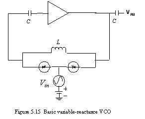
           Generally, a variable-reactance type of voltage-controlled oscillator is used in FM applications. The variable-reactance VCO uses the varactor diode as a voltage-variable capacitance, as illustrated in figure 5.15, where the capacitance is varied with the modulation voltage, Vm.

Basic variable reactance VCO
" Frequency Modulation " !

The Superheterodyne AM Receiver


A block diagram of a superheterodyne AM receiver is shown in figure 5.12. The receiver shown consists of an antenna, an RF (radio frequency) amplifier, a mixer, a local oscillator (LO), an IF (intermediate frequency) amplifier, a detector, an audio amplifier, a power amplifier, and a speaker.

A block diagram of a superheterodyne AM receiver


    Antenna                                                            

    The antenna picks up all radiated signals and feeds them into the RF amplifier. These signals are very small (usually only a few microvolts).

    RF Amplifier                                                   
     This circuit can be adjusted (tuned) to select and amplify any carrier frequency within the AM broadcast band. Only the selected frequency and its two side bands pass through the amplifier. (Some AM receivers don't have a separate RF amplifier stage.)

    Local Oscillator                                              
   This circuit generates a steady sine wave at a frequency 455 KHz above the selected RF frequency.

    Mixer                                                               
    This circuit accepts two inputs, the amplitude modulated RF signal from the output of the RF amplifier (or the antenna when there is no RF amplifier) and the sinusoidal output of the local oscillator (LO). These two signals are then "mixed" by a nonlinear process called heterodyning to produce sum and difference frequencies. For example, if the RF carrier has a frequency of 1000 KHz, the LO frequency is 1455 KHz and the sum and difference frequencies out of the mixer are 2455 KHz and 455 KHz, respectively. The difference frequency is always 455 KHz no matter what the RF carrier frequency.


    IF Amplifier                                                     
    The input to the If amplifier is the 455 KHz AM signal, a replica of the original AM carrier signal except that the frequency has been lowered to 455 KHz, The IF amplifier significantly increases the level of this signal.

    Detector                                                           
   This circuit recovers the modulating signal (audio signal) from the 455 KHz IF. At this point the IF is no longer needed, so the output of the detector consists of only the audio signal.

    Audio and Power Amplifiers                         
   This circuit amplifies the detected audio signal and drives the speaker to produce sound.

Signal flow through an AM receiver

" The Superheterodyne AM Receiver " !

Signal Quantization


Consider an analog signal whose values from 0 to +10.let us assume that we whish to convert this signal to digital form and that the required output is a 4-bit digital signal .we know that a 4-bit binary number can represent 16 different values, 0 to15: it follows that the resolution of our conversion will be 10V/15=2/3V.thus an analog signal of 0V will be represented by 0000.2/3V will be represented by 0001, 6V will be represented by 1001, and 10V will be represented by 1111.
All these sample numbers are multiples of the basic increment (2/3V).A question now arises regarding the conversion of numbers that fall between these successive incremental levels. For instance, consider the case of a 6.2-V analog level. This process is called quantization. Obviously errors are inherent in this process; such errors are called quantization errors. Using more bits to represent(encode or, simply, errors code) an analog signal reduces quantization  errors but requires more complex circuitry.
" Signal Quantization " !

Friday, June 10, 2011

Amplitude Demodulation


The linear multiplier can be used to demodulated or detect and AM signal. Demodulation can be thought of as reverse modulation. The purpose is to get back the original modulating signal (sound in the case of standard AM receivers). The detector in the AM receiver can be implemented using a multiplier, although another method using peak envelope detection is common


     The Basic AM Demodulator                                  
An AM demodulator can be implemented with a linear multiplier followed by a low pass filter, as shown in figure 5.7 The critical frequency of the filter is the highest audio frequency that is required for a given application (15 KHz, for example)
Basic AM demodulator
Figure 5.7 Basic AM demodulator.


      Operation in Terms of the Frequency Spectra
Let's assume a carrier modulated by a signal tone with a frequency of 10 KHz is received and converted to a modulated intermediate frequency of 455 KHz, as indicated by the frequency spectra in figure 5.8. Notice that the upper side and lower side frequencies are separated from both the carrier and the IF by 10 KHz.


AM signal converted to IF
Figure 5.8 An AM signal converted to IF
When the modulated output of the IF amplifier is applied to the demodulator along with the IF. Sum and difference frequencies for each input frequency are produced as shown in figure 5.9. Only the 10 kHz audio frequency is passed by the filter.  A draw back to this type of AM detection is that a pure IF must be produced to mix with the modulated IF.
Example of demodulation
Figure 5.9 Example of demodulation.


         IF and Audio Amplifiers                


     The basic function of the IF Amplifier
 The IF amplifier in a receiver is a tuned amplifier with a   specified bandwidth operating at a center frequency of 455 KHz for AM and 10.7MHz for FM. The IF amplifier is one of the key features of a super heterodyne receiver because it is set to operate at a signal resonant frequency that remains the same over the entire band of carrier frequency that can be receiver. Figure 5.10 illustrates the basic function of an IF amplifier in terms of the frequency spectra.
          Assume, for example. That the received carrier frequency of     ƒc=1MHz is modulated by an audio signal with a maximum frequency of ƒm=5 KHz indicated in the following figure.
IF Amplifier in AM Receiver


By the frequency spectrum on the input to the mixer for this frequency, the local oscillator is at frequency of


                         ƒo = 1MHz + 455KHz = 1.455MHz


The mixer produces the following sum and difference frequencies as indicated in the previous figure.


                ƒo + ƒc = 1.455MHz + 1MHz = 2.455MHz  
                ƒo – ƒc = 1.455MHz – 1MHz = 455KHz
      ƒo + (ƒc + ƒc) = 1.455MHz + 1.005MHz = 2.46MHz
      ƒo + (ƒc – ƒc) = 1.455MHz + 0.995MHz = 2.45MHz
      ƒo – (ƒc + ƒc) = 1.455MHz – 1.005MHz = 450KHz
     ƒo – (ƒc – ƒc) = 1.455MHz – 0.995MHz = 460KHz


Since the IF amplifier is a frequency-selective circuit, it responds only to 455 KHz and any side frequencies lying in the 10 KHz band centered at 455 KHz. So, all of frequencies out of the mixer are rejected except the 455KHz IF, all lower-side frequencies  down to 450 KHz, and all upper-side frequencies up to 460 KHz. This frequency spectrum is the audio modulated IF.
The audio amplifier in a receiver system
Figure 5.11 The audio amplifier in a receiver system.
" Amplitude Demodulation " !

Modulation/Demodulation Circuits

The purpose of a communication system is to transmit information-bearing signals through a communication channel separating the transmitter from the receiver. Information-bearing signals are also referred to as baseband signals. The term baseband is used to designate the band of frequencies representing the original signal as delivered by a source of information. The proper use of the communication channel requires a shift of the range of baseband frequencies into other frequency ranges suitable for transmission, and a corresponding shift back to the original frequency range after reception.


For example, a radio system must operate with frequencies of 30 KHz and upward, whereas the base band signal usually contains frequencies in the audio frequency range, and so some form of frequency band shifting must be used for the system to operate satisfactorily. A shift of the range of frequencies in a signal is accomplished by using modulation, which is defined as the process by which some characteristic of a carrier is varied in accordance with a modulating wave (signal). A common form of the carrier is a sinusoidal wave, in which case we speak of a continuous-wave modulation process. The baseband signal is referred to as the modulating wave, and the result of the modulation process is referred to as the modulated wave. Modulation is performed at the transmitting end of the communication system. At the receiving end of the system, we usually require the original baseband signal to be restored. This is accomplished by using a process known as demodulation, which is the reverse of the modulation process.

         In basic signal-processing terms, we thus find that the transmitter of an analog communication system consists of a modulator and the receiver consists of a demodulator, as depicted in figure 5.1, In addition to the signal received from the transmitter, the receiver input includes channel noise. The degradation in receiver performance due to channel noise is determined by the type of modulation used.


Modulator and Demodulator
In this chapter we study two families of continuous-wave (CW) modulation systems, namely, amplitude modulation and angle modulation. In amplitude modulation, the amplitude of the sinusoidal carrier wave is varied in accordance with the baseband signal. In angle modulation, the angle of the sinusoidal carrier wave is varied in accordance with the baseband signal.

 
" Modulation/Demodulation Circuits " !

The A/D and D/A Converters as Functional Blocks


Fig 4.3 depicts the functional block representations of A/D and D/A converters. As indicated, the A/D converter (also called an ADC) accepts an analog sample VA and produces an N-bit digital word. Conversely, the D/A converter (also called a DAC) accepts an N-bit digital word and produces an analog sample. The output samples of the D/A converters are often fed to a sample-and-hold circuit. At the output of the S/H circuit a staircase waveform, such as that in Fig 4.4, is obtained. The staircase waveform can then be smoothed by a low-pass filter, giving rise to the smooth curve shown in the next figure. In this way an analog output signal is reconstructed. Finally, note that the quantization error of an A/D converter is equivalent to +/- 1/2 least significant bit (bs).


Converters Circuit Block


Fig 4.4 The analog samples at the output of a D/A converter are usually fed to a sample-and-hold circuit to obtain the staircase waveform shown. This waveform can then be filtered to obtain the smooth waveform. The time delay usually introduced by the filter is not shown.


" The A/D and D/A Converters as Functional Blocks " !

Why Data Converters?


        Our environment is full of analog signals, such as sound, light, temperature, voltage, current, and electromagnetic waves. By the use of sensors, these signals are usually converted to electrical quantities, voltage or current, and processed to extract useful information. The processing can be carried out in analog or digital domain. During the last two decades, digital signal processing has become immensely powerful. Advances in technology of Integrated Circuits (IC) made it possible to implement digital signal processors with a reasonable amount of silicon wafer area, low power consumption, and affordable price for different applications. Digital signal processors (DSP) can easily be programmed for different algorithms. Many functions of analog circuits have been replaced by equivalent algorithms in DSPs. Another major advantage of DSP algorithms is that functionality is not subjected to fluctuations and variations with respect to time and temperature.


 In addition, there are some functions that can be performed by DSP, but are difficult to implement with analog circuits. One such function is a linear phase filter. The main advantages of DSP over analog processing are programmability, repeatability, stability, and flexibility.
 
         Although an increasing amount of signal processing is performed in digital domain, the interface between analog and digital domain will remain a fundamentally necessary element. The gates of DSPs to analog signals are Analog-to-digital (A/D) and Digital-to-Analog (D/A) converters. For example, an echo cancellation in an amphitheater makes use of a microphone that generates a voltage in the range of a few microvolts to a couple of milivolts. This analog voltage should be amplified and converted to a digital signal for extensive processing by DSP. After echo cancellation, it is converted to an analog signal, which can be applied to a power amplifier.


Fig 4.1

  
" Why Data Converters? " !

Data Converter


Analog-to-digital (A/D) and digital-to-analog (D/A) converters are needed in all digital signal processing (DSP) applications and act as the interface between the analog and digital signal. As DSP continues to gain ground over analog signal processing, the importance of these converters increases correspondingly. The high-speed and high-resolution A/D converters are required in numerous applications, such as wireless communications, asymmetric digital subscriber line (ADSL), and very high-speed DSL (VDSL) systems.
       Sampling rate and precision or bit resolution greatly controls the performance of the data converters. In general case, we deal with a trade-off between these criteria. Different types of converter architectures offer system designers a wide range of choice in speed and resolution for optimal use in their applications. Among the choices in A/D architectures are flash, pipeline, successive-approximation register (SAR), and sigma-delta converters. D/A architectures include resistor-string converters, current-mode converters, and sigma-delta converters. Among these, sigma-delta converters are widely used in high-resolution applications.


         In addition, the test of the data converters is becoming even more important issue in mixed signal applications. The test of A/D and D/A converters can be carried out by using a DSP unit. In each case, some practical DSP solutions for the state-of-the-art-applications are given by using Texas Instruments (TI) data converters and DSP products.
" Data Converter " !

Amplitude Modulation ( AM )


Amplitude modulation is used since the first days of the 20th century mainly for transmitting voice and signals through the conventional broadcast band like the long-, medium- and short wave bands because of its easy and cheap way of realisation.
Besides the consumption of bandwidth in comparison to usual FM is relatively small and the receivers could be made up very simple.


AM Signal


Standard AM system
Standard AM system

AM is an important method for transmitting information. We shall state the circuits used in the modulation and demodulation of the AM signals.

References
 
" Amplitude Modulation ( AM ) " !

CMOS NOR gate

The realization of a two-input CMOS NOR gate is shown Fig 4.4. For the  NOR gate, The output should be low when either input A or input B is high. Thus the NMOS portion of the gate is identical to that of the NMOS NOR gate. However, in the CMOS gate, we must ensure that a static current path does not exist through the logic gate, and this requires the use of two PMOS transistors in series in the PMOS transistor network.

CMOS NOR circuit diagram
Fig 3.4. NOR circuit diagram.


The complementary nature of the conducting paths can be seen in Table 3.3.A conducting path exists through the NMOS network for V1 = 1 or V2 =1 However, a path exists through the PMOS network only when both V1 = 0 and V2 = 0 (no conducting path through the NMOS network).


(a)


 (b)


 (c)


Fig 3.5. NOR input output voltages. (a) Input voltage (v1) (b)  Input voltage (V2)
        (c)  Output voltage (Vout)
Table 3.3   CMOS NOR Gate Truth Table and Transistor States


CMOS NOR Gate Truth Table and Transistor States


" CMOS NOR gate " !

Circuits Used in the Amplitude Modulation

Amplitude and Balanced Modulation

Amplitude modulation is a technique which uses a low-frequency signal to control the amplitude of a high- frequency signal. A simple modulator can be constructed using a multiplier as shown in figure 5.2.

Figure 5.2 A simple amplitude modulator circuit.


One input is the high-frequency or carrier signal, and the other input is the modulating signal. A sinusoidal source at a frequency of 10 kHz is used to represent the carrier signal and a second source at a frequency of 1 kHz is used to represent the modulating signal. Notice that the peak amplitude for the carrier is set to 1 volt using the parameter VcarrierPK. The modulating index is the ratio of the peak of the modulating signal to the peak of the carrier. Here, the index is set to 0.8 or 80% modulation. A typical broadcast AM signal includes the carrier as well as the sidebands in the transmission. To get such a double sideband transmitted carrier signal (DSB-TC) we must bias or offset the modulating signal by a value equal to the carrier's peak voltage. The amplitude modulated signal and the modulating signal from this simulation are shown in figure 5.3.
Figure 5.3 An amplitude modulator output signal.


      A balanced modulator produces a double sideband suppressed carrier signal (DSB-SC). By setting the offset of the modulating signal to be zero in the above circuit, we will suppress the carrier. Notice, the output of this modulator shown in figure 5.4; the shape of its upper A balanced modulator output signal envelope resembles a full-wave rectified AC source.
Figure 5.4 A balanced modulator output signal


     By using a specific OTA                       
    ( Operational transconductance amplifier )
      The LM13700 is a typical OTA and serves as a representative device. The LM13700 is a dual-device package containing two OTAs and buffer circuits. Figure 5.5 shows the pin configuration using a single OTA in the package. The maximum dc supply voltages are +18v and  -18v .
 For an LM13700, the bias current is determined by the following formula:


The 1.4 v is due to the internal circuit where a base-emitter junction and a diode connect the external Rbias with the negative supply voltage (-V). The positive bias voltage, +Vbias, may be obtained from the positive supply voltage, +V.


 Fig. 5.5
    Two OTA Applications                   
Amplitude modulator…….Figure 5.6 illustrates an OTA connected as an amplitude modulator. The voltage gain is varied by applying a modulation voltage to the bias input. When a constant-amplitude input signal is applied, the amplitude of the output signal will vary according to the modulation voltage on the bias input. The gain is dependent on bias current, and bias current is related to the modulation voltage by the following relationship:


This modulating action is shown in fig 5.6 for a higher-frequency sinusoidal input voltage and a lower-frequency sinusoidal modulating voltage.


The OTA as an amplitude modulator


Figure 5.6 The OTA as an amplitude modulator.
     References
     
" Circuits Used in the Amplitude Modulation " !

How to Convert Analog Signal Into Digital One


In order to make analog to digital conversion we should convert the analog signal into digital by sampling and quantization processes ( Pulse Code Modulation) .


         Sampling of Analog Signals                    
       The principle underlying digital signal processing is that of sampling the analog signal Fig 4.2 illustrates in a conceptual form the process of obtaining samples of an analog signal. The switch shown closes periodically under the control of a periodic pulse signal (clock). The closure time of the switch, τ, is relatively short, and the samples obtained are stored (held) on the capacitor. The circuit of the following figure is known as a sample-and-hold (S/H) Circuit. As indicated, the S/H circuit consists of an analog switch that can be implemented by a MOSFET transmission gate. A storage capacitor, and (not shown) a buffer amplifier.
Between the sampling intervals-that is, during the hold intervals-the voltage level on the capacitor represents the signal sample we are after. Each of these voltage levels is then fed to the input of an A/D converter, which provides an N-bit binary number proportional to the value of signal sample. The fact that we can do our processing on a limited number of samples of an analog signal while ignoring the analog-signal details between samples is based on the shannon’s sampling theorem


Fig 4.2  The process of periodically sampling an analog signal (a) Sample-and-hold (S/H) circuit The switch closes for a small part of time of every clock period (T). (b) Input signal waveform. (c) Sampling signal (control signal for the switch). (d) Out put signal (to be fed to A/D converter).

" How to Convert Analog Signal Into Digital One " !