Custom Search

Wednesday, May 11, 2011

Inverter Delay Time and Power Dissipation


The inverter delay time can be calculated as follows


Fig. 3.a shows inverter delay time as a function of the channel length. It shows that the delay time decreases as the channel length decreases.


Variation of the inverter delay time as a function of channel length
Fig. 3.a. Variation of the inverter delay time as a function of channel length 


The inverter power dissipation can be expressed as follows


Fig. 3.b shows the variation of the inverter power dissipation as a function of supply voltage. The power dissipation decreases as the supply voltage decreases.
Variation of the inverter power dissipation as  a function of supply voltage
Fig. 3.b. Variation of the inverter power dissipation as  a function of supply voltage.


" Inverter Delay Time and Power Dissipation " !

Inverter


The CMOS logic gate can be conceptually modeled by the circuit in Fig 3.1, in which the position of the two switches is controlled by the input voltage vi. The circuit is designed so there will never be a conducting path between the positive and negative power supplied under steady –state conditions. When the NMOS transistor is on, the PMOS transistor is off; if the PMOS transistor is on, the NMOS device is off.
CMOS Inverter circuit diagram
Fig 3.1. Inverter circuit diagram


In the CMOS inverter of Fig 3.1,  the source of the PMOS transistor is connected to VDD , the source of the NMOS transistor is connected to VSS (0 V in this case), and the drain terminals of the two MOSFETs are connected together to form the output node. Also the substrates of both the NMOS and PMOS transistors are connected to their respective sources, and so body effect is eliminated in both devices.

CMOS Inverter input voltages

(a)

CMOS Inverter output voltages
 (b)

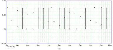
Fig 3.2.  Inverter input output voltages, (a) Input voltage.  (b) Output voltage

Table 3.1 CMOS Inverter truth table and transistor states
CMOS Inverter truth table and transistor states

    CMOS Voltage Transfer characteristics            
Figure 3.3 shows the voltage transfer characteristic (VTC) of the Symmetrical CMOS inverter, designed with Kp=KN . The VTC can be divided into five different regions, as shown in the figure and summarized in table 3.2. For an input voltage less than VTN = 1V in region 1, the NMOS transistor is off, and the output is maintained at VOH = 5V by the PMOS device.
Similarly, for an input voltage greater than (VDD - | VTP | )(4 V) in region 5, the PMOS device is off, and the output is maintained at V0L = 0V by the NMOS transistor. In region 2, the NMOS transistor is saturated, and the PMOS transistor is in the linear region. In region 3, both transistors are saturated. The boundary between regions 2&3 defined by the boundary between the saturation and linear region of operation for the PMOS transistor. Saturation of the PMOS device requires:
Table 3.2 Regions of operation of transistors in a symmetrical CMOS inverter
Regions of operation of transistors in a symmetrical CMOS inverter

In a similar manner, the boundary between regions 3 and 4 is defined by saturation of the NMOS device:
 
In region 4, the voltage place the NMOS transistor in the linear region, and the PMOS transistor remains saturated. Finally, for the input voltage near VDD/2   (region 3), both transistors are operating in the saturation region.
By using small channel length, produce increase in cut – off frequency so delay time decreased and this increase speed of operation.
Also me advantages of using small channel length:
1- decreasing tsohreshold voltage
2- decreasing supply voltage
3- decreasing palter dissipation
" Inverter " !

CMOS Logic Circuits


For many years, complementary MOS (CMOS) technology was available only in unit logic form, with several gates packaged together in a single dual in – line package (DIP), but it was not widely used in complex integrated circuits. CMOS requires that both NMOS and PMOS transistors be built into the same substrate, and the increased complexity and cost this represents were the primary reasons why CMOS technology was little used .as time passed ,however ,the size of transistors in ICs continued to decrease, so an ever – larger number of gates could be placed on a given size IC chip. By the early 1980s, the total power consumption of NMOS ICs was becoming prohibitive. The problem was so severe that it was hampering progress in increasing the density of ICs. To solve the static power dissipation problem, the microprocessor industry at this point rapidly moved to CMOS technology. Today, CMOS is the industry wide standard technology.
This chapter investigates the design of CMOS logic circuits, starting with characterization of the CMOS inverter, and follows with a discussion of the design of NOR,NAND,and complex gates  based on  CMOS reference inverter . 

" CMOS Logic Circuits " !

Operation with a DiFFerential Input Voltage


Next we apply a difference or differential input voltage by grounding the gate of Q2  (i.e.,setting vG2 = 0) and applying a signal vid to the gate of Q1 as shown in Fig. 2.3. It is easy to see that since vid=vGS1-vGS2 , if vid is positive, VGSl will be greater than vGs2 and hence iD1 will be greater than iD2 and the difference output voltage (vD2-vD2) will be positive. On the other hand, when vid is negative, vGS1 will be lower than vGS2 , iD1 will be smaller than iD2, and correspondingly vD1 will be higher than vD2; in other words, the difference or differential output voltage (vD2-vD1) will be negative.
The MOS differential pair with a differential input signal

Fig. 2.3  The MOS differential pair with a differential input signal vid applied. With vid  positive: vGS1 > vGS2 , and vD1<vD2 thus thus (vD2-vD1) will be positive. With vid negative: vGS1 < vGS2, iD1< iD2 and (vD1>vD2­ ) thus (vD2-vD1) will be negative.

From the above, we see that the differential pair responds to difference-mode or differential input signals by providing a corresponding differential output signal between the two drains. At this point, it is useful to inquire about the value of vid that causes the entire bias current I to flow in one of the two transistors. In the positive direction, this happens when vGS1 reaches the value that corresponds to   iD1= I, and vGS2 is reduced to a value equal to the threshold voltage Vt, at which point vs=-Vt The value of vGS1 can be found from


where VOV  is the overdrive voltage corresponding to a drain current of 1/2 (Eq. 2.5). Thus the value of vid at which the entire bias current I is steered into Q1 إس

if vid is increased beyond  
 , iD1 remains equal to I, vGS1 remains equal to
, and vS rises correspondingly, thus keeping Q2 off. In a similar manner we can show that in the negative direction, as vid  reaches 
 ,Q1 turns off and Q2 conducts the entire bias current I.
Thus the current I can be steered from one transistor to the other by varying vid din the range
  
 
which defines the range of differential-mode operation. Finally, observe that we have assumed that Q1 and Q2 remain in saturation even when one of them is conducting the entire current I.
To use the differential pair as a linear amplifier, we keep the differential input signal vid small. As a result, the current in one of the transistors (Q1   when vid is positive) will increase by an increment  
 proportional to vid  to
Simultaneously, the current in the other transistor will decrease by the same amount to become    
A voltage signal 
 develops at one of the drains and an opposite-polarity signal, 
, develops at the other drain. Thus the output voltage taken between the two drains will be 
 , which is proportional to the differential input signal vid. The small-signal operation of the differential pair .

The MOSFET differential pair for the purpose of deriving the transfer      characteristics
 
FIGURE 2.5 The MOSFET differential pair for the purpose of deriving the transfer      characteristics, iD1 and iD1 versus vid=vG1 -vG2 .
" Operation with a DiFFerential Input Voltage " !

Operation with a Common-Mode Input voltage

To see how the differential pair works, consider first the case of the two gate terminals 
interjoined together and connected to a voltage vCM called the common-mode voltage. That is as shown in Fig (2.2)                
 
Since Ql and Q2 are matched, it follows from symmetry that the current I will divide equally between the two transistors. Thus
and the voltage at the sources, vs will be

 
where VGS is the gate-to-source voltage corresponding to a drain current of I/2. Neglecting channel-length modulation, VGs and I/2 are related by


or in terms of the overdrive voltage   
  
                                                                                                                             
The voltage at each drain will be

Thus, the difference in voltage between the two drains will be zero.

The MOS differential pair with a common-mode input voltage
Fig. 2.2      The MOS differential pair with a common-mode input voltage

Now, let us vary the value of the common-mode voltage vCM Obviously, as long as Q1 and Q2 remain in the saturation region, the current I will divide equally between Q1 and Q2 and the voltages at the drains will not change. Thus the differential pair does not respond to (i.e., it rejects) common-mode input signals.
       An important specification of a differential amplifier is its input common-mode range.This is the range of vCM over which the differential pair operates properly. The highest value of vCM is limited by the requirement that Q1 and Q2 remain in saturation, thus

The lowest value of vCM is determined by the need to allow for a sufficient  voltage across current source I for it to operate properly. If a voltage Vcs is needed across

the current source, then


" Operation with a Common-Mode Input voltage " !

The MOS Differential Pair


Figure 2.1 Shows the basic MOS differential-pair configuration. It consists of two matched transistors, Q1 and Q2 whose sources are joined together and biased by a constant-current source I . The latter is usually implemented by a MOSFET circuit. For the time being, we assume that the current source is ideal and that it has infinite output resistance. Although each drain is shown connected to the positive supply 
The basic MOS differential-pair configuration
 
Fig 2.1  The basic MOS differential-pair configuration

through a resistance RD, in most cases active (current-source) loads are employed, as will be seen shortly. For the time being, however, we will explain the essence of the differential pair operation utilizing simple resistive loads. Whatever type of load is used, it is essential that the MOSFETs not enter the triode region of operation.

References
 
" The MOS Differential Pair " !

Tuesday, May 10, 2011

Differential Amplifier


     The differential-pair or differential-amplifier configuration is the most widely used building block in analog integrated-circuit design. For instance, the input stage of every op amp is a differential amplifier. Also, the BJT differential amplifier is the basis of a very-high-speed logic circuit family called emitter-coupled logic (ECL). Initially invented for use with vacuum tubes, the basic differential-amplifier configuration was subsequently implemented with discrete bipolar transistors. However, it was the advent of integrated circuits that has made the differential pair extremely popular in both bipolar and MOS technologies. There are two reasons why differential amplifiers are so well suited for IC fabrication: First, as we shall shortly see, the performance of the differential pair depends critically on the matching between the two sides of the circuit. Integrated-circuit fabrication is capable of providing matched devices whose parameters track over wide ranges of changes in environmental conditions. Second, by their very nature, differential amplifiers utilize more components (approaching twice as many) than single-ended circuits. Advantage of integrated-circuit technology is the availability of large numbers of transistors at relatively low cost.
Nevertheless it is worthwhile to answer the question: Why differential? Basically, there are two reasons for using differential in preference to single ended amplifiers.
The First, differential circuits are much less sensitive to noise and interference than single-ended circuits. To appreciate this point, consider two wires carrying a small differential signal as the voltage difference between the two wires. Now, assume that there is an interference signal that is coupled to the two wires, either capacitively or inductively. As the two wires are physically close together, the interference voltages on the two wires will be equal. Since, in a differential system, only the difference signal between the two wires is sensed, it will contain no interference component!

The second reason for preferring differential amplifiers is that the differential configuration enables us to bias the amplifier and to couple amplifier stages together without the need for bypass and coupling capacitors such as those utilized in the design of discrete-circuit amplifiers. This is another reason why differential circuits are ideally suited for IC fabrication where large capacitors are impossible to fabricate economically. As will be seen the design and analysis of differential amplifiers makes extensive use of the material on single-stage amplifiers .We will follow explain of differential amplifiers with examples of multistage amplifiers. The section concludes with two SPICE circuit simulation examples.
" Differential Amplifier " !

Wireless Communications


During the past few years, there has been an exponential growth in cellular telephone and pager market. In the next generation, the wireless data will be part of the communication systems. The DSP is the core of data processing unit. The application of D/A and D/A Converters in typical cellular phone is shown in Fig 1.7. It is seen that there are two different sets of data converters: voice-band data converters and high sampling rate at the radio frequency (RF) modulator. The voice band requires a low sampling (8KHz) but relatively high resolution, e.g., 13 bits. The RF section requires relatively high-speed but not high resolution, e.g. 8 bit.
The circuit designers prefer to integrate more functionalities in DSP part rather than in analog part. It results in lower number of components and in turn lower overall cost. The strategy of more integration in DSP part depends on the achievable specifications of high speed and high-resolution data converters with low  power implementation for portable applications.

Wireless Communications Block Diagram
Fig 1.7 Wireless Communications

 
" Wireless Communications " !

CMOS vs Cost Reduction

      
  Cost reduction is a major tenet of CMOS. The primary factor underlying the decreasing cost per circuit is the increase in density, or circuits per square millimeter. The cost of processing a silicon wafer must increase much less rapidly than the density in order to achieve cost reduction. The rapid (25% per year) increase during the 1980s of the capital cost of a silicon manufacturing line led to concerns of diminishing returns in cost per circuit. However, since 1990 the rate of increase has slowed to less than 15% a year. Major factors behind this reduction were a stabilization of clean-room requirements, better equipment productivity and utilization, and a slower increase in the number of process steps. The dominant cost factor in producing integrated circuits is the capital cost for the clean-room building and the equipment. The rate of increase of these costs must be matched by a greater rate of increase of components per chip. As long as the increase in components per chip is utilized by effective designs providing more function for the user, the industry will continue to thrive.
" CMOS vs Cost Reduction " !

High Performance Logic Technology and Reliability Challenges


Power Trend
Fig 1.3 Power growing due to increased operating frequency and increased transistor count.

The remarkable characteristic of transistors that fuels the rapid growth of the information technology industry is that their speed increases and their cost decreases as their size is reduced. The only other product in manufacturing with this characteristic over such a vast range of size reduction is the hard disk drive with magnetic storage. The transistors manufactured today are 20 times faster and occupy less than 1% of the area of those built 20 years ago. It seems intuitively obvious that


continued reduction of the area of a transistor by a factor of 2 every three years cannot be sustained forever. However, predictions of the limit of size reduction or even of the pace of size reduction As shown in Fig 1.5 have proven to elude the most insightful prognosticators. The predicted “limit” has been dropping at nearly the same rate as the size of the transistors. The accuracy of a prediction of the future of CMOS technology is therefore not likely to be very great. However, the key principles underlying the evolution of CMOS technology can give us some insight into the future.

Fig 1.4 We find the increase in number of transistor

Fig 1.5 Reduction in size


Fig 1.6 Increase in frequency response


We find from this figure :

Logic Technology Evolution

Each new technology generation provides:

1)  Size scaling decrease by 1.42 .

2)  Increase in transistor density by 2.

3) Increase transistor switching speed by 1.5.

4) Reduced chip power.

5) Reduced chip cost.

 
" High Performance Logic Technology and Reliability Challenges " !

Future Directions


Microprocessors are essential to many of the products we use every day such as satellite, televisions, cars, radios, home appliances, and, of course, computers. Transistors are the main components of microprocessors. At their most basic level, transistors may seem simple. But their development actually required many years of painstaking research. Before transistors, computers relied on slow, inefficient vacuum tubes and mechanical switches to process information. In 1958, engineers (one of them Intel co-founder Robert Noyce) managed to put two transistors onto a silicon crystal and create the first integrated circuit, which led to the microprocessor.
The first microprocessor to make it into a home computer was the Intel 8080, a complete 8-bit computer on one chip, introduced in 1974. The first microprocessor to make a real splash in the market was the Intel 8088, introduced in 1979 and incorporated into the IBM PC (which first appeared around 1982). If you are familiar with the PC market and its history, you know that the PC market moved from the 8088 to the 80286 to the 80386 to the 80486 to the Pentium to the Pentium II to the Pentium III to the Pentium 4. All of these microprocessors are made by Intel and all of them are improvements on the basic design of the 8088. The Pentium 4 can execute any piece of code that ran on the original 8088, but it does it about 5,000 times faster!
As shown in Table 1.4 helps you to understand the differences between the different processors that Intel has introduced over the years. From this table you can see that, in general, there is a relationship between clock speed and MIPS. The maximum clock speed is a function of the manufacturing process and delays within the chip. There is also a relationship between the number of transistors and MIPS. For example, the 8088 clocked at 5 MHz but only executed at 0.33 MIPS (about one instruction per 15 clock cycles). Modern processors can often execute at a rate of two instructions per clock cycle. That improvement is directly related to the number of transistors on the chip and will make more sense in the next section.


             Table 1.4  Intel processor technologies over the years

Intel processor technologies over the years


  • Data Width is the width of the ALU. An 8-bit ALU can add/subtract/multiply/etc. two 8-bit numbers, while a 32-bit ALU can manipulate 32-bit numbers. An 8-bit ALU would have to execute four instructions to add two 32-bit numbers, while a 32-bit ALU can do it in one instruction. In many cases, the external data bus is the same width as the ALU, but not always. The 8088 had a 16-bit ALU and an 8-bit bus, while the modern Pentiums fetch data 64 bits at a time for their 32-bit ALUs.
  • MIPS stands for "millions of instructions per second" and is a rough measure of the     performance of a CPU. 

References 

" Future Directions " !

Ballistic Transport


Ballistic Transport means that carriers will travel faster than the average drift velocity or the saturation velocity, and this effect can lead to very fast device. Ballistic transport  will occur in ( L < 1um ).
The frequency response of MOSFETs increases as the channel length decrease as shown in Fig 1.6,


            Fig.1.2 shows the device circuit parameter as a function of the channel length. Table 1.3 illustrates the scaling factor k as a function of the circuit parameters. Typically,  k ~ 0.7 per generation of a given technology.


       Table 1.3 device circuit parameter as a function of the scaling factor.

Device circuit parameter as a function of the scaling factor
                                                       
CMOS logic technologies

Fig 1.2 History and trends of power-supply voltage (VDD ), threshold
voltage (Vt ), and gate-oxide thickness (tox) vs. channel length for
CMOS logic technologies.

References     

" Ballistic Transport " !

Typical Values of MOSFET Parameters


Typical values for the important parameters of NMOS and PMOS transistors fabricated in a number of CMOS processes are shown in this Table 1.2.

Table 1.2 parameters of NMOS and PMOS transistors

Parameters of NMOS and PMOS transistors


As indicated in Table, the trend has been to reduce the minimum allowable channel length. This trend has been motivated by the desire to pack more transistor on a chip as well as to operate at higher speeds or, in analog terms, over wider bandwidths. Although the magnitudes of the threshold voltages Vtn and Vtp have been decreasing with Lmin, from about 0.7 ~ 0.8 V to 0.4 ~ 0.5 V, the reduction has not been as large as that of  the power supply VDD. The latter has been reduced dramatically, from 5V for older technology to 1.8 V for .18µm. This reduction has been necessitated by the need to keep the electric fields in the smaller devices from reaching very high values.
Another reason for reducing VDD is to keep power dissipation as low as possible given that the IC chip now has a much larger number of transistors. We find high cut frequency response of the common-source amplifier and higher operating speeds and wider amplifier bandwidths than the longer device, for example, see that  for a 0.25-µm NMOS transistor can be as high as 10 GHz.

a)   Advantages
1)  The major advantages of silicon gate CMOS ICs are their higher speed and lower power consumption. These features impact a broad range of device performance parameters. A faster chip widens the scope of possible applications and increases signal quality and reliability. For a given frequency response, power can be reduced. The CMOS ICS can respond to higher frequency inputs, the timers can oscillate at higher frequencies, and the response times of operational amplifiers and comparators are reduced while slew rate and operating frequency increase. All of these qualities give wider signal frequency range and operating and design margin providing increased accuracy and gain bandwidth at reduced voltages and power requirement over broad operating conditions.

2)   The low power consumptions of CMOS chips is advantageous in a number of different ways. Many devices can operate at supply voltages as low as 1V and with ultra low leakage current which facilitates battery operation. This not only means less power consumption, but for operational amplifiers and comparators it results in a lower offset voltage caused by thermal drift and for timers it results in higher accuracy and stability. This lessens the dependence of timing accuracy on expensive components, increasing the accuracy and reducing the cost of the timing function. In addition, as the number of transistors per chip increases, the low power consumption of CMOS Ics allow greater densities but will require little or no external cooling and very little self-heating design considerations.
3)   Another advantage of silicon gate CMOS linear technology to be discussed here is its compatibility with CMOS digital technology. The availability and relative ease with which digital functions such as logic gates, flip-flops, counters and memory cells can be added to the analog library means that complete systems, including a large amount of digital logic, analog modules, and passive components such as resistors and capacitors, can all be integrated into one ASIC chip. This capability is referred to as mixed mode (analog and digital) integration where most components of an electronic system are implemented in a single monolithic IC chip. Generally, in a given system only a few other types of components such as transducers, sensors, inductors, precision resistors, large capacitors, relays, etc. are left off the IC chip.

4)    The final advantage of CMOS linear technology is high circuit function density as shown in Fig 1.4 and low cost. As CMOS linear technology is a VLSI (very large scale integration) technology, many circuit function blocks can be integrated onto the same monolithic IC chip, not only producing compactness, and system miniaturization, but also producing low per function cost and high per function reliability. Furthermore, due to integration of large number of elements, board area cost, labor cost and inventory management costs are greatly reduced.
" Typical Values of MOSFET Parameters " !